The Evolution of Global Semiconductor Manufacturing and the Expanding Role of the Photoresist Market
The semiconductor industry has undergone a radical transformation over the past decade, driven by the relentless pursuit of miniaturization and increased processing power. At the heart of this technological revolution lies the chemical foundation of microelectronics: the photoresist. This light-sensitive material is essential for photolithography, the process used to etch intricate circuit patterns onto silicon wafers. As consumer demand for smarter, faster, and more efficient electronic devices grows, the industry is witnessing a significant surge in Photoresist Market analysis as stakeholders seek to understand the complexities of chemical formulations and their compatibility with next-generation extreme ultraviolet lithography. The shift toward 5G technology, artificial intelligence, and high-performance computing has necessitated the development of advanced chemically amplified resists that can achieve sub-7nm nodes. This progress is not merely a technical milestone but a fundamental shift in how electronic components are conceived and manufactured, requiring deep collaboration between chemical suppliers and semiconductor foundries to ensure that the material properties align with the thermal and mechanical demands of modern chip architecture.
The broader implications of these material advancements extend into various sectors, including automotive electronics, telecommunications, and healthcare technology. Modern vehicles, now equipped with sophisticated sensor arrays and autonomous driving capabilities, rely on chips produced using high-purity photoresist materials. As the industry moves toward more sustainable manufacturing practices, there is a growing emphasis on reducing the environmental impact of photoresist processing by developing greener solvents and more efficient stripping agents. Market participants are increasingly focusing on the integration of specialty chemicals that offer better resolution, sensitivity, and etch resistance to minimize defects during the manufacturing cycle. This focus on quality control and material innovation is pivotal for maintaining high yields in semiconductor fabrication plants. Furthermore, the geographical concentration of semiconductor manufacturing in the Asia-Pacific region continues to shape supply chain strategies, prompting global players to invest heavily in regional R&D centers to stay ahead of the competition and respond to the rapidly changing needs of the global electronics ecosystem.
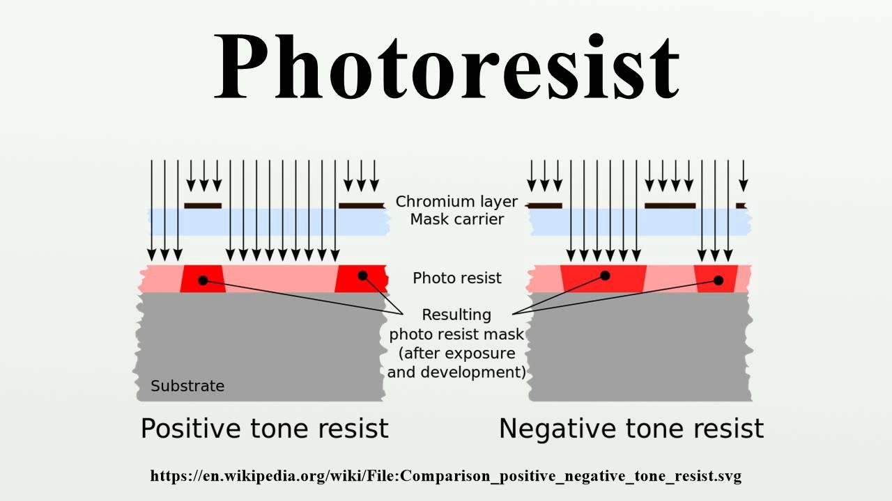
What are the primary types of photoresists used in modern electronics? Photoresists are generally classified into positive and negative types; positive resists become soluble when exposed to light, while negative resists become insoluble, each serving different resolution requirements in chip fabrication.
How is the transition to EUV lithography affecting the market? Extreme Ultraviolet (EUV) lithography requires specialized photoresists with high sensitivity to shorter wavelengths, driving significant investment in new chemical formulations to achieve smaller feature sizes on silicon wafers.
➤➤➤Explore MRFR’s Related Ongoing Coverage In Semiconductor Industry:
Reconfigurable Intelligent Surfaces Ris Hardware Market
Advanced Metering Infrastructure Market
Ground Penetrating Radar Market
Non-Destructive Testing Services Market
4 Inches Semi Insulating Silicon Carbide Wafer Market
Electric Vehicle Battery Management System Market
Fingerprint Recognition Ceramic Cover Market
Categorias
Leia Mais
The North America Wastewater Reverse Osmosis (RO) Membrane Market is a critical contributor to the global water treatment industry, driven by technological innovation, strict environmental regulations, and increasing demand for water reuse solutions. Reverse osmosis membranes are widely utilized across municipal and industrial sectors in North America to remove contaminants, improve water...
Latest Insights on Executive Summary India Menstrual Cups Market Share and Size CAGR Value The India menstrual cup market is expected to reach USD 27.38 million by 2033 from USD 15.43 million in 2025, growing with a substantial CAGR of 7.6% in the forecast period of 2025 to 2033 The market insights gained through this keyword market research analysis report facilitate a more defined...
Key Drivers Impacting Executive Summary Biosensors Market Size and Share CAGR Value Global biosensors market was valued at USD 24.60 billion in 2022 and is expected to reach USD 54.21 billion by 2030, registering a CAGR of 9.30% during the forecast period of 2023 to 2030. The Biosensors Market report contains market insights and analysis for Biosensors Market industry, which are...
Despite the rapid advancement of laser technology in 2026, tattoo removal in Dubai is still surrounded by outdated information and urban legends. Many people hold onto the past—remembering the days of aggressive lasers and patchy results—and allow these myths to prevent them from seeking the clear skin they desire. At Tajmeels Clinic, we believe that an informed patient is a...

Introduction to PRP Hair Regeneration Hair loss affects millions, leaving many in Riyadh searching for reliable solutions. PRP Hair Treatment in Riyadh emerges as a popular, natural option using your own blood plasma to stimulate follicles. This regenerative therapy draws from platelet-rich plasma (PRP), packed with growth factors that promote hair regrowth. Unlike invasive surgeries,...